Case Study: Follow These 10 Steps to Develop Your Electronic Product. Let’s Start from Brainstorming Session…

In this article, Dennis will share his experience years ago participating a practical project from concept to production: The development of a consumer electronic product. Briefly to use 10 steps to explain how it was made, from concept, sketching, prototype, molding and all the way to mass-production.

Step 1         Brainstorming

Brainstorming session

Once the project is off the ground, project manager/leader will call a meeting the participants including sales, marketing, designer, engineer to contribute their experiences or comments. I realized some people commented design thinking is better qualified to explore users’ unmet need rather than brainstorming session. Steve Jobs even said, “We do no market research.” Dennis personally see Steve Jobs as God in mind, dare not to challenge his achievements. Anyhow let’s put the argument aside and see how other people did by using the method of brainstorming.

The leader of brainstorming is crucial, their attitude or leading skill will decide whether the meeting is success or not. The leader should inspire the participants with passion to evoke varieties of creative ideas, less interference and free from the limitation of technology. I will not focus on brainstorming here, more discussion will be left in other chapter about PM, Product management.

Step 2         Converging the imaginative ideas into product specification

Concepts to specifications

Most of the ideas proposed by participants in brainstorming are wild. Good idea always meaning customers are interested to buy-in. But in the brainstorming make no pre-judge to those ideas are crucial.

Step 3         Building Function Block Diagram and developing hardware, software and firmware

Function block diagram
Circuit diagram

The function block diagram is the fundamental of the whole device/system to be developed. With the diagram, the E/E, Electrical engineer will have a whole picture among main board, wireless module, power board of your system. Once the structure is confirmed, the following step is to develop circuit diagram then gerber out for PCB manufacturing.

Step 4         Concept development and sketching

Design sketching
Design sketching

After brainstorming session, the product manager organizes those proposed ideas into MRS, Marketing Requirement Specification document. Following, the industrial designers start creating design concepts as much as they can base on MRS using variety of drawing tools, e.g. pigment pen, marker, color pencil…etc. taking balance between forms and functions.

Step 5         3D Model & rendering

Normal people without design degree or trained to “imagine” the essential of 2D sketches. 3D modeling technique today is very realistic to simulate real things in life than before. Creo, Solidworks, UG, Alias, Rhino…are all popular in the market to build any kind of free-form surface. Once 3D model is built the outer dimension of the product also decided.

Thanks to the modern rendering technology, industrial designer is hundred times easier to finish a realistic outcome using professional tool like V-Ray or Keyshot than before. Any color, material, texture or lighting all just at a click.

Step 6         Mechanical engineering

Mechanical engineering

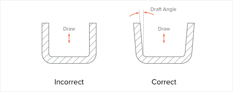
The 3D model created by industrial designer can’t be applied for manufacturing because it is not the major task to consider if the design conforms with the need from manufacturing point of view. Next, now is the show time for mechanical engineer. They deeply care if the parts could be molded or shaped and if the parts are robust enough to resist the harsh use in real scenario. Adding ribs, draft angle, snaps, boss, groove, wall thickness, all must be well considered in this stage. Industrial designer concerns about usability, and mechanical engineer cares about functionality and reliability.

Step 7         Prototype

CNC Prototyping

Working prototype is the only/effective way for potential users, buyers or even angels to touch-and-feel your concept before it officially goes mass-production. Once the 3D CAD completed by mechanical engineer, the factory is able to manufacture those parts whatever they are plastic or metal using CNC machine. In real process, the factory engineer will re-organize the way to build the parts according to his experience using less material and time to minimize the cost the customer would happy to afford. After the parts are CNC milled, following step the technician will polish, refine then painting by following the CMF documents we repeatedly mentioned earlier. Finally, you can assemble the PCBA (PCB Assembly with all electrical components on PCB) together with enclosures then you have a working prototype to live-demo to whom interests to your project.

Step 8         Molds development

LEGO Brick molds

Most modern consumer products use thermoplastics. In process, the heated molten plastic is injected into the space formed by the cavity-side and core-side of the mold under high pressure and high speed through molding machine. There are kinds of steel used for mold, such as: S50C, P20, NAK80 (pre-hardened steel) or SUS420 (stainless steel), etc. The standard process to build the molds including CNC, wire-cut, EDM (Electro-discharge machining), fine-tuning, polishing and final assembly. Product designers can assign any specific area of the product surface with different textures using MOLD-TECH texture template which is well-known global standard in industry.

Step 9         Molding

Molding
Injection machine

Step 10       Assembly and mass-production

EMS, Electronics Manufacturing Service

In 21st century, the assembly line for mass-production invented by Ford Motor Company, founded in 1927 still proves working well today. The labor follows the SOP to make assembly step by step in preset station. The advantage of applying assembly line is every worker can get same result as others do long as you fully follow the SOP. In industry, you can rely on the EMS, Electronic Manufacturing Service to make FATP, Final Assembly Test & Packing for product mass-production.

It’s an annoying journey to go through the whole hardware development process from concept all the way to production. But you are not alone, you can find many materials like articles, classes, videos on-line to self-learning. Congratulations! you have a whole picture about developing an electronic product now, what’s your next step? Take an action of course.

References link

Recommend hardware accelerator
https://hax.co/
https://bolt.io/
http://highway1.io/
https://www.plugandplaytechcenter.com/

More contents about hardware innovation to share with you, stay tuned!
Email contact: dennis.you@tw-mpi.com

How to Deal with Molds Maker?

Learn to deal with mold factory

Most of the leaders of hardware startups are EE, Electrical Engineering background, without the knowledge for supply-chain management especially for mechanical parts. Dennis worked for molding factory for years, he will show you some tips how to deal with mold factory. With these basics, you will have more understanding to know their language, working process and terminology. At least, you will no longer look like a fool when you talk to them.

Molds (sometimes called tooling) with varieties of forms. In this article let’s focus on plastic injection mold. Once you have the whole picture, it will be very helpful for you to understand other kinds of molds which are made in different technologies. Because they have similar process/concept in common, e.g. metal diecasting.

Here are some key terminologies you should know before going further:

  1. CMF: Color, Material & Finish
  2. Cavity
  3. Family mold
  4. Mold material
  5. Draft angle
Pantone Color Formula Guide

Significant terminology about molding

1. CMF: Color Material & Finish

CMF is a document for describing the basic characters of the parts. Colors are diversity, you can pick any color you want from Pantone Color Formula Guide for your parts appearance.

Most of the mold makers they have Pantone Color Formula Guide, this is a very commonly used tool worldwide.

Material stands for what kind of resin is used for your plastic parts. Very commonly to be mentioned in industry are: ABS, PC/ABS, PMMA (acrylic), POM, Nylon, TPU…etc. All with its strength/advantage for your applications.

Finish, meaning you must decide how the parts look like from outer appearance. Normally there three grades: Glossy (mirror polish), Matte, Textured. It is highly relevant with mold material you use for your molds. Let’s discuss this in later articles.

2. Cavity

It’s easy to understand what cavity means if you ever made pancake at home using the machine like this:

Mold cavity

From the photo you can see on top of the machine, a metal tray with 25-cavity for your pouring batter into the cavities. When the batter is cooked you get 25 pancakes done at a time. We can say this is a multi-cavity mold. Same concept to your mold, we must decide how many cavities will be made before molds start to build. It is relevant to your mold investment and to the unit cost of the parts as well. Less cavity less mold investment but also high in unit cost, vice versa.

3. Family mold

For cost-saving consideration in the beginning of your business, sales volume is still unpredictable. Using family-mold is smart choice. You can put those parts with different shape but the material and color must be same. Once resin injected, you can get many parts in a injection cycle time. See following photo.

Family mold

4. Mold material

Injection mold

Before your molds start to build, we need to discuss the molds specifications with factory. This is crucial as it is highly connected with budget investment. There are several kinds of molds material to choice e.g. S50C, P20, NAK80, SUS420, Starvax…etc. If the parts surface requested for glossy, the hardness of mold material is as hard as possible, like NAK80, Starvax. Normally P20 is best balance between quality and cost-effectiveness for most of the applications for consumer electronics or IoT products.

5. Draft angle

To make the part from ejection mold easier, a draft angle must be added to all vertical walls. Walls without a draft angle will have drag marks on their surface, due to the high friction with the mold during ejection. A minimum draft angle of 2° is recommended. Larger draft angles (up to 5o °) should be used on taller features.

Draft angle

References link

Injection Molding
https://www.3dhubs.com/guides/injection-molding/

More contents about hardware innovation to share with you, stay tuned!
Email contact: dennis.you@tw-mpi.com

Who Comes First When Developing a Hardware Product? Industrial Designer or Electrical Engineer?

Dennis was always asked same question when he was mentoring hardware startups: Who comes first when developing a hardware product? Industrial designer or electrical engineer?

I am pretty sure this issue bothers most of the startup teams. According to Dennis experience, a lot of startups they go ID, industrial design first. Because they can request designer to develop sexy sketches and 3D renderings, putting them on presentation to catch more attentions from angels or venture capital. Even they don’t have any POC, Proof of concept or demo board to show their technology. With these design drawings the project is more look like close to commercial production stage, not staying in concept stage. 

The short-cut to bypass the mine-field

The answer is clear and simple. If you never develop similar product/technology before, it’s better to start from electrical engineering. Let’s do it inside-out.

You are still working on electrical issues, meaning your key components will be changed, replaced very fast in one single day. You are not able to estimate what the PCB size might be. In that case, industrial designer can’t give you a reasonable dimension for enclosure. They develop those ideas freely without any constrain. The result those designs look sexy also junk to you, the PCBA can’t fit with form-factor perfectly. This in not what you want.

The secret recipe guiding you how to cook delicious meal looks like this:

Step 1
EE starts to build a demo-board to simulate the optimized electrical circuits to be developed.

Step 2
EE estimates the true PCB size according to demo board and handovers it to product designer. They will start to develop concept design base on the PCB size you offer.

Step 3
ID issues PCB 2D outline drawing for EE’s layout. Enclosure design also follows same PCB size as reference to build 3D model. Then the industrial designer (ID), mechanical engineer (ME) and electrical engineer (EE) have to co-working together to get the integrate everything. Everybody stays on same page to go through the whole product developing process.

Step 4
Everybody will be very busy from now. The industrial designer keeps working on design details to get an eye-catching sexy design for market.

The mechanical engineer starts to add necessary structures for plastic or metal parts molding e.g. rib, boss, snap, thickness, draft angle…etc.

Electrical engineer processes for block diagram, PCB layout, electrical diagram, gerber file, and making it into a PCBA which stands for PCB Assembly. PCBA is made by SMT or DIP equipment, mounting or welding all electrical components on PCB bare board.

Conclusions

Dennis make the conclusion simpler:
Build it from inside-out. If your new product to be developed is relevant with IoT then EE is always the core, everything should start from here. Find a tool kit like Arduino or Raspberry Pi or making your own demo board to validate all functions you need. When all tests are done, you will figure out what PCB assembly size might be for future and what parts are going to be listed in BOM, meaning Bill of Material. In that case, industrial design can run before electrical, engineering without any problem at all.

References link

IDEO: A global design company. We create positive impact through design.
https://www.ideo.com/

Design and innovation that transforms.
https://www.frogdesign.com/

How a Hardware Product Was Developed? This Short Video Might Answer Some Questions in Your Mind.

From 0 to 1 to mass-production

In this video, you will realize how a hardware product was made. Everything starts from a sketch in very beginning. In this stage, the ID means industrial designer will help you to build a sexy outlook for your product. They use professional skill to develop hundreds of sketches and building some potential ideas into 3D using software e.g. Alias, Rhino, CREO, SOLIDWORKS….and Keyshot or V-Ray are for real-time rendering.

From Product Design to Working Prototype

When industrial design lock-down, the ME guy mechanical engineer starts to develop mechanism for all parts. This is for next stage to make prototypes for POC, Proof of Concept or production molds.

Another key route is EE, electrical engineer will create circuit diagram, PCB layout. In the end, using SMT facility to put all electronic components onto PCB to produce PCB assembly.

Now you have plastic enclosures made by CNC-made, and you have PCB assembly. This is the first time you can put all parts together into a working prototype. So far, you already achieved from 0 to 1 from rough concept all the way to physical working prototype. Now it’s the time to relax? Not yet, you are still far away from success.

Expanding Your Funding and Orders Using Working Prototype

Once you hold a working prototype in hand, you can go to crowdfunding to get more funding, hold a meeting with angels or venture capital or knock door to retail channels for volume orders. As a team leader, these are what you should focus at this moment, not sit down and enjoy a tea-time.

If you are lucky, dragging lots of attention from VC or Kickstarter now you have money and orders. You are preparing to go to next level: mass-production. But your nightmare is also coming to negotiate/cooperate with single factory or the whole supply-chain. We will leave this critical issue to later chapters to talk about.

Mass-production is a form of art. Accompanying along with technology, science, statistic or even negotiation power. Let’s temporarily assumed the FedEx plane already loading your quality products and take off from the airport. So far you have earned your first barrel of golds.

References Link

METRO PRODUCTS INC.
http://www.metroproducts.com.tw/

More contents about hardware innovation to share with you, stay tuned!
Email contact: dennis.you@tw-mpi.com

Hardware Is Hard. Who Said So?

This article is to give hardware startup team a whole picture where are they standing and where to go in the journey of developing new hardware products.

Hardware is hard, but not that hard.

Even your dear mom went to Costco to prepare delicious meals for families, she still finds it a challenging job. In fact, there are some basic rules to follow to develop a hardware product. Here In this blog, Dennis will reveal you some techniques from his pocket. The development of a hardware product, from the very beginning idea to mass production, we can divide it into two stages:
1. POC, Proof of Concept proof of concept
2. MP, Mass-production
The challenges that start-up teams faced in these two phases are extremely different.

How it’s made?

From 0 to 1, get your first POC ready

POC, Proof of Concept refers to from 0 to1. A concept that has been in your mind for a long time and turns it into a set of model/mockup/prototype that can represent your original ideas. Once done, such a rough prototype is no longer ambiguous for storytelling. It can be touched and felt from engineering point of view. However, the set of Proof of concept is just good enough for R&D team to see the whole picture, to take reference for the next step of optimization and improvement.

Once the Proof of concept is complete, the next step is to optimize it. This optimization process is called EVT, Engineering Verification Test. Because this POC uses the materials around you and might be Ardunio development board is used (if you know coding as well), most of the cases are: ugly, the casing is broken, the circuit is easily disconnected, and you can’t take it to see the potential customers or the angels who may be interested in your project, consumers are even less likely to spend money on your junk, and you have to quickly rebuild it and make it looks as sexy as possible. Now you have to co-work with external resources to make this happen. At this moment, you need at least four professionals to assist you:
1. ID, Industrial designer, or product designer
2. ME, Mechanical engineer
3. EE, Electrical engineer
4. PM, Product manager

Through the collaboration of above professional designers, engineers, and PMs, at this stage of EVT, we completed the sexy appearance, mechanical structure that meets mass production requirements, and size-optimized PCB. Appearance and function, both beautiful and operable. It looks like a working prototype very close to commercial production. With this set of functional models, start-up teams can start doing the following things that might with chance to change your whole life:
1. Go to make a crowdfunding video.
2. Go to potential angels to raise funds.
3. Go to buyers for order.

From DVT stage, preparing for mass-production

After the completion of EVT, there are stages such as DVT, PVT, MP…etc. There are different levels of challenges waiting for the startups team. We will not reveal too much implementation details in this article, let everyone have a whole picture of how hardware product is developed. Simply put, this article is like a subway map to let the startups team know: Where they are now? Where is the next stop and where should they get off the train. With future blog posts, more details will be revealed for your reference.

As mentioned earlier, Dennis has an industrial designer background, has been a product manager for 10+ years, is the head of international marketing and business departments, and has served in the mold injection molding factory in past 20 years career. After setting up his own company, it is committed to providing global hardware startups from 0 to 1 to mass production service and has many years of practical experience. The posts in this blog are all original created by Dennis. He is delighted for sharing his painstaking with everyone here.

References Link

Notes on Marty Cagan’s Root Causes of Product Failure
https://walkerux.wordpress.com/2016/09/03/notes-on-marty-cagans-root-causes-of-product-failure/

EVT v. DVT v. PVT Explained
https://news.ewmfg.com/blog/evt-dvt-pvt-explained

More contents about hardware innovation to share with you, stay tuned!
Email contact: dennis.you@tw-mpi.com

使用 WordPress.com 設計專業網站
立即開始使用